Researchers paint portrait of Marie Curie in semiconductor
Novel technique for spatially controlled deposition of semiconductors within one single layer
13 April 2021
In the paper, Helmbrecht and Noorduin present their novel ion-exchange lithography technique that takes on the fundamental challenge of patterning semiconductor materials with different properties in a single film. This patterning is essential for the development of next‐generation (opto)electronic functional components such as LEDs or solar cells.
The concept of the novel technique is to use a reactive 'ink' that can be painted or printed on an equally reactive 'canvas', after which a perovskite semiconductor forms by means of ion exchange. As a demo, the researchers used the technique to airbrush an image of Madame Curie.
Colourful technique
Perovskites are a new and highly promising class of semiconductor materials for the fabrication of LEDs, solar cells and other optoelectronic devices. In their Marie Curie demo, the researchers created a perovskite by taking a layer of lead carbonate as their canvas and a solution of methylammonium bromide as their ink. The latter undergoes a chemical reaction with the lead carbonate to form a perovskite emitting green light. Choosing different inks enables the creation of many different perovskites. For instance, using solutions containing other halides instead of bromides allows to paint blue- or red-emitting perovskite patterns matching the green pattern - or to airbrush or print even more complex patterns.
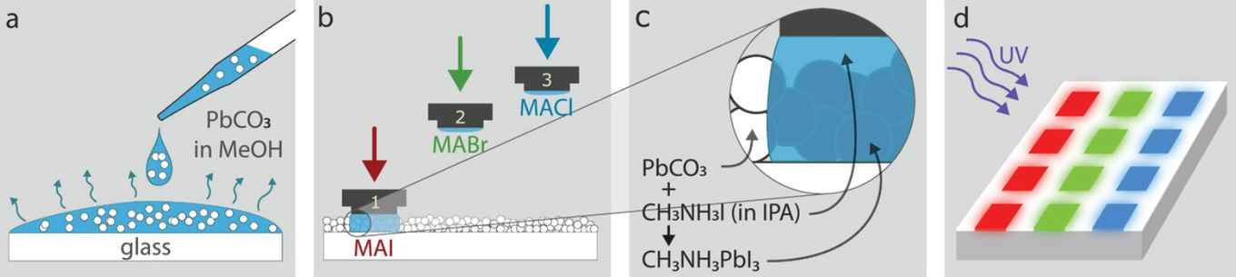
The research has demonstrated that the patterns can be created very accurately: drops of ink just a few micrometres in size yield perovskite dots of also just a few micrometres in size. This means the ink does not run. “The challenge of this research was developing the chemical reaction and the conditions: the quantity of ink, the pressure, and the properties of the canvas. None of these was known, and the process does not work if they are not exactly right,” says Helmbrecht.
Different perovskites in one single layer
The new ion exchange lithography is fundamentally different from existing techniques for depositing perovskite layers, Helmbrecht explains. “All traditional techniques result in different layers of different perovskites. Our method results in one single layer that consists of different types of perovskite.” In addition, perovskites are usually quite sensitive to the treatments used in traditional methods, such as etching or rinsing. These can damage the perovskite. With ion exchange lithography, such treatments are no longer needed. “We have developed a far simpler method for applying a pattern of different perovskite semiconductors next to each other on a chip or LED,” Helmbrecht says. Cleanrooms or other special conditions are no longer required. The researchers have already demonstrated the utility of ion exchange lithography by using the technique to produce a working LED. “That has proven the principle.”
Paper
L. Helmbrecht, M.H. Futscher, L.A. Muscarella, B. Ehrler, W.L. Noorduin, Ion Exchange Lithography: Localized Ion Exchange Reactions for Spatial Patterning of Perovskite Semiconductors and Insulators, Advanced Materials (2021). DOI: 10.1002/adma.202005291
Links
AMOLF press release: Painting with semiconductors.
Website Van 't Hoff Institute for Molecular Sciences.